Detection of X-ray and Gamma-ray
Photons Using Silicon Diodes
Detection Technology, Inc.
Micropolis, Finland
December, 2000
Direct Detection in Silicon -- DC Current Mode
Direct detection of X-ray and Gamma-ray photons in Silicon utilizes PIN diodes with a relatively thick active (wholly or partially depleted) region, as exemplified by the XRA, XRB, and PDC-series of devices from Detection Technology, Inc.
When x-ray or gamma ray photons penetrate the active region of a PIN diode, some (or in certain cases all) of the photons' kinetic energy may be absorbed through interactions with bound electrons resulting in ionization -- liberation of unbound charge in the form of hole-electron pairs.
3.6 eV of gamma or x-ray photon energy absorbed in silicon are required to liberate one electron-hole pair. The holes (+ charges) drift toward the anode, and the electrons (- charges) drift toward the cathode under the influence of an internal electric field which is directed across the diode junction from cathode to anode.
This electric field arises -- even in the absence of any external applied voltage -- from a concentration gradient of donor and acceptor atoms at the interface between P-type and N-type material, and results in the well-known built-in junction voltage (1)(~0.6V) which is typical of silicon diodes. In some applications, an additional, external back-bias may be utilized to augment this built-in voltage.
The (+) and (-) charges drift in opposite directions, summing together to form a current which, in turn, can be measured with the aid of an external amplifying circuit.
Example 1: Calculate the current produced in a Si PIN diode for 1000 MeV per second of absorbed energy from x-ray or gamma ray photons.
Solution: 3.6 eV of gamma or x-ray photon energy absorbed in silicon are required to liberate 1 electron-hole pair.
(109 eV / sec) ÷ (3.6 eV per electron-hole pair) x
(1.6 x 10 -19 coulombs per electron-hole pair) = 4.444 x 10 -11 amperes.
But 1000 MeV / sec = 1.6 x 10⁻¹⁰ watts
Thus, the responsivity, expressed in amperes per watt for x-ray or gamma ray photons absorbed in Si is:
(4.444 x 10 -11 amperes) ÷ (1.6 x 10⁻¹⁰ watts) = 0.2777 amperes per watt.
Spectral Responsivity

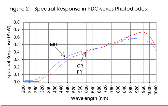
Fig. 2: Spectral Responsivity for PDC-series Photodiodes
Figure 2 (above) shows the response in amperes per watt for light of different wavelengths incident on PDC-series PIN photodiodes. The two curves are for different entrance window materials. A wavelength of 1100 nm (just beyond the extreme right side of the graph) corresponds to a photon energy of 1.12 eV, below which photons cannot excite electrons into the conduction band. Thus, silicon "goes blind" at wave-lengths of 1100 nm and longer.
Compare the value (0.277 amperes per watt) for the responsivity for penetrating x-rays or gamma-rays, found earlier, with the spectral responsivity for photons in the visible and infra-red portion of the spectrum, shown in Fig. 2 for PDC-series photodiodes.
Dose and Dose Rate
In many applications it is dose or dose rate, rather than absorbed energy that is the quantity of interest. Dose is defined as Energy absorbed per unit mass. Dose rate is defined as energy absorbed per unit mass per unit time. The standard SI unit for dose is the joule per kilogram, which has been named the gray.
Example 2: Calculate the current produced in a DTI type PDC-24S-CB diode (2.4 mm x 2.4 mm x .380 mm thick) for a dose-rate in Si of 1 gray per hour.
Solution:
Volume = .24 x .24 x 0.038 = .00219 cm3
Density (of Silicon) = 2.336 g / cm3
Mass of active region = .00219 x 2.336 = .00511 g = .00000511 Kg
Dose-rate = 1 joule / (Kg 3600 sec) = .00028 joule / (Kg sec)
Rate of energy absorption, or "Power" absorbed in diode =
[.00028 joule / (Kg sec)] x [0.00000511 Kg] =
1.43 x 10 -9 joules / second , or 1.43 x 10⁻⁹ watts
Current (per gray per hr in a 2.4 mm x 2.4 mm x .38 mm thick diode) =
[0.2777 amperes per watt] x [1.43 x 10⁻⁹ watt] = 3.97 x 10⁻¹⁰ amperes
An older unit of dose, the rad, (100 ergs per gram) is still in wide use. One gray equals 100 rads, so that:
Current = 3.97 x 10⁻¹² amperes per rad hr-1 in a 2.4 mm x 2.4 mm diode.
In round numbers, this is ~0.7 pA per (rad / hour) per square mm.
Or 70 pA per (gray / hour) per square mm.
Response to external radiation
In many applications a measurement of the intensity of an external radiation field, rather than an explicit measure of absorbed dose or dose-rate in the diode, is required. In radiation protection applications, the intensity of the external radiation field is termed exposure dose-rate and is commonly expressed in units of roentgens per hour. The roentgen is defined as an amount of x-ray or gamma radiation which produces 3.33 x 10⁻¹⁰ coulombs of electronic charge in 1 cm3 of air at standard temperature and pressure.
Calculating the current-response to an external radiation field is somewhat more complicated than the previous examples, since both the probability of photon interaction in the silicon diode (detection efficiency) and the amount of energy deposited per photon interaction are complex functions of photon energy.
For the moment, we shall define detection efficiency rather loosely as the ratio (x 100%) of the number of photons which deposit some (as yet undetermined) energy in our diode, divided by the total number of photons which are incident on the face of the Si diode. For direct detection in a Si PIN diode (i.e., without the use of a scintillating screen or crystal) the detection efficiency is a function of the thickness of the silicon wafer, as shown in Fig. 3 below. For a wafer thickness of 380 microns (the thickness which is now used in DTI's standard line of diode products) the detection efficiency is close to 100% at 10 KeV, falling to approximately 1.60% at 100 KeV.
The curves shown in Fig. 3 below are for the Si wafer only, and do not take into account any effects due to the window, substrate, or package in which the diode is mounted. At low energies (below ~30 KeV), photon interactions in Si are primarily photo-electric. For energies above approximately 60 KeV, photons interact in Si almost entirely through Compton scattering.
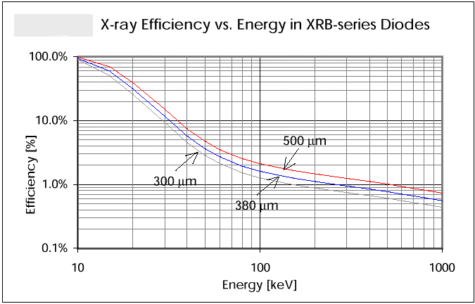
Figure 3
Example 3: Calculate the DC-current response for a 20 mCi point-source of ß+ - emitting activity (gamma-ray energy = 511 KeV annihilation radiation) at a distance of 10 cm from a type XRB-24S-CB PIN diode detector.
Solution:
Let A = area of the diode in cm2 = .057 cm2
N = flux of incident gamma rays (gamma's / second-cm2 on face of diode)
r = detection efficiency at 511 KeV = .0077 from Fig. ___.
Ê = average energy of recoil electrons in Si detector, expressed in eV
s = ionization constant in silicon = 3.6 eV / electron-hole pair
e = electronic charge = 1.6 x 10⁻¹⁹ coulombs
Then the average current produced in the diode is given by:
I = N A r Ê e / s
In this example, two 511 KeV gamma rays are emitted back-to-back from the source for each ß+ event. The photon flux at the detector is: N = (2 x 20 x 3.7 x 107) / (4 x 10² ) = 1,177,740 gamma photons / cm2-second. This is equivalent to an exposure dose-rate at the face of the diode of ~1.08 roentgens / hour. An exact expression for the average energy of a Compton recoil electron may be found in (2). An approximate formula -- accurate enough to be useful over a wide range of gamma ray energies (3) -- is given by Ê = 1/2 Emax, where Emax is derived from Compton's formula for the energy of the 180o (back-scattered) photon: (4)
Emax = h {2 hv / (m0c2 + 2 hv)} = energy of the back-scattered photon
hv = the energy of the incident photon (expressed in eV)
m0c2 = 511,000 eV
In this example hv = 511,000 eV, so that Emax = 340,000 eV, and Ê = 170,000 eV. Therefore, the radiation - induced current in the diode = 1,177,740 x .057 x .0077 x 170,000 x 1.6 x 10-19 / 3.6 = 3.90 x 10⁻¹² amperes.
Notice that, in this example, an exposure dose-rate of ~ 1 roentgen per hour produces approximately the same current in the diode as an absorbed dose-rate (i.e., energy absorbed in Si) of 1 rad per hour. This generally holds for gamma ray energies above ~100 KeV, where Compton interactions predominate within materials of relatively low atomic number (as in the constituents of human tissue).
The scale factor relating total charge to exposure dose for this example is:
(3.90 x 10⁻¹² amperes) x (3600 seconds per hour) / (1.08 roentgens per hour), or
1.30 x 10⁻⁸ coulomb / roentgen.
One roentgen produces, by definition, 3.33 x 10⁻¹⁰ coulombs in 1 cm3 of air at standard temperature and pressure. Thus, our XRB-24S-CB diode (.057 cm2 x 380 microns thick) produces approximately the same radiation-induced current as a (1.30 x 10⁻⁸) / (3.33 x 10⁻¹⁰ ) = 39 cm3 standard air-ionization chamber.
The effect of the window and device packaging
Some sort of "window" is always required on the face of the diode to maintain chemical passivation of the surface of the silicon. Even a "window-less" diode must have such protection in the form of a very thin aluminum or silicon nitride layer. At very low photon energies, the thickness and type of material used for the window can introduce substantial attenuation, as shown in figures 4 and 5 below.
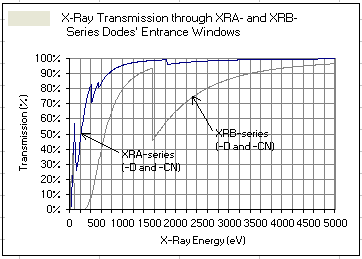
Fig. 4
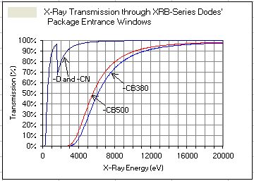
Fig. 5
If the diode is mounted in some sort of package (which is almost always the case) the active region of the diode is in electronic equilibrium with the surrounding medium comprising the diode package, substrate, window and outer coating, etc., so that at higher gamma energies Compton recoil electrons which are produced near -- and close enough to penetrate -- the active volume of the diode, are also detected. For this reason the overall effective volume (or equivalently, the overall, effective efficiency) at 100 KeV and above may actually be somewhat greater than shown in fig. 3.
Amplifying small currents
For dose-rates encountered in laboratory monitoring or general survey applications, the radiation-induced photo-current produced in Si diodes normally ranges between ~10-12 and ~10-8 amperes. Such small currents demand particular care in the design and implementation of amplifying circuitry.
Utilizing the diode's terminal voltage is generally not advisable, since the diode voltage is a logarithmic rather than linear function of dose-rate. In order to preserve linearity of response, the diode must be connected across a very low-resistance circuit. For this reason, diode current is almost always measured with the aid of a transimpedance amplifier (current-to-voltage converter).
A transimpedance amplifier is generally implemented as a high-gain, inverting amplifier (usually in the form of an integrated-circuit operational amplifier) with a feedback resistor connected from output to input, as shown in Fig. 6 below. This particular example shows the photodiode with its cathode grounded (+ current flowing into the amplifier) producing a negative voltage at the output of the amplifier. High forward gain forces the voltage at the amplifier's inverting input to be essentially zero, thus satisfying the requirement for low resistance across the diode.
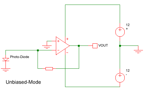
Fig. 6
Assuming the amplifier's open loop gain is sufficiently high (Av >106), the transimpedance gain of this circuit is just the value of the feedback resistor, in ohms. Thus, for example, a 100 megohm feedback resistor provides a gain of 108 ohms (1 volt output for 10-8 amperes input).
Speed of response
Some applications, such as pulsed X-ray measurements, require precise measurement of rapidly-varying signals. A system rise-time response in the micro-second range, or faster, requires that the diode be operated in biased mode in order to maintain a low junction capacitance, and also to insure rapid and complete collection of all the available charge - particularly the holes -- which drift more slowly than electrons. Biased - mode operation is illustrated in Fig. 7 below.
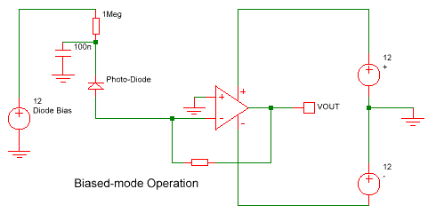
Fig. 7:
Both junction capacitance and leakage current or dark current are functions of reverse bias, as illustrated in Figs. 8 and 9 below.
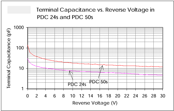
Fig. 8
Dark Current
Dark current is also a very strong function of temperature, increasing by a factor of ~2 for every 5-6 deg. C increase in temperature. Since dark current cannot readily be distinguished from radiation-induced photo-current, it may become a significant source of error when undertaking low-level radiation measurements. This is particularly true if the temperature is not held constant (a back-biased Si diode makes a highly sensitive -- albeit non-linear -- thermometer!)
Guard Ring
Leakage current in a planar diode generally comprises three components: 1) a current component flowing fully vertically in the depletion region of the diode, 2) a component due to the edge-field of the depletion region, which is generated just outside the true active area and, 3) a component due to surface effects in the oxide layer. This last component is one which is most heavily affected by radiation damage in the silicon / silicon dioxide interface outside the active area, and is also strongly affected by temperature changes.
The magnitude of the dark current can be reduced by exploiting DTI's unique, proprietary guard ring. This feature is particularly useful when operating in biased mode; the guard ring collects most of the latter two components of dark current (noted above), and thereby decreases the dark current by approximately a factor of 0.5.
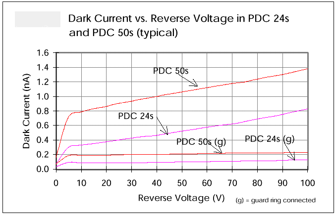
Fig. 9
Another advantage of the guard ring is that it reduces potential gradients at the edge of the diode's active area, thereby increasing the breakdown voltage rating. A third advantage becomes important in spectroscopic applications (to be covered in more detail in a subsequent tutorial) wherein the guard ring collects most of the signal charge which is generated close to -- or outside of -- the actual active area, reducing the number of interactions in which imperfect or incomplete charge collection would otherwise occur.
Compare the respective values of dark current (for the same device and the same reverse bias) with the data in Fig 9 in which the guard ring was not used. Equally dramatic is the comparison between different devices; A 5 x 5 mm diode (PDC-50S) with the guard ring connected shows less than half the leakage current compared to a 2.4 x 2.4 mm diode (PDC-24S) whose guard ring is not connected!
The circuit connection for the guard ring is shown in the schematic in Fig. 10. Please observe that the cathode of the diode is common to both the main diode and the guard ring. Therefore, the guard ring is useful only when the cathode is connected to a positive voltage supply, and the input of the preamplifier is connected to the anode of the diode. We strongly recommend this configuration. (Some users prefer connecting to the cathode since that provides a positive signal output from an inverting amplifier. However, in most applications, this will result in poorer performance.)
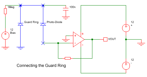
Fig. 10
Amplifier Offset
If high-speed response is not required, then errors due to dark current are substantially reduced by operating the diode radiation detector in unbiased mode. However, there is yet an additional confounding factor which must be taken into account: the amplifier's input offset-voltage error.
Unless precisely and specifically "trimmed out", some degree of input offset error is present in virtually all amplifiers. Offset voltage error is represented schematically as a voltage source in series with the (+) input terminal of the amplifier. In our transimpedance amplifier (fig. 6 & fig. 10), this offset voltage is returned via the feedback resistor so as to appear at the (-) input terminal of the amplifier.
Thus, the "unbiased" diode is not actually operating at zero bias, but rather at a small positive or negative bias (depending on the polarity of the offset voltage) which is on the same order as the amplifier's offset voltage and which, in turn, introduces a finite dark-current component.
Shunt Resistance
Potentially much more serious is the effect of the diode's shunt resistance. The quotient of (voltage ÷ current) at a diode bias V = 10 mV is defined as the device's shunt resistance. If the value of the diode shunt resistance is substantially less than the value of the transresistance amplifier's feedback resistor, then the voltage gain of the amplifier, referred to the (+) input terminal is approximately: (Rshunt + Rfeedback) / (Rshunt)
Example 4: Estimate a transresistance amplifier's output voltage assuming the following:
1) doserate = 0
2) diode shunt resistance = 100 megohms
3) operational amplifier offset voltage = 1 mV, and
4) amplifier feedback resistor = 109 ohms
Solution: The output voltage error (for zero doserate) is dominated by the amplifier's offset error voltage multiplied by the gain of the amplifier referred to the (+) input terminal....
Vout = Voffset x (Rshunt + Rfeedback) / (Rshunt) =
(.001) x (109 + 108) / (108 ) = 0.011 volts
This is equivalent to an input offset current (at zero doserate) of 11 pA in the diode detector.
Worse yet, dark current is a very strong function of temperature as we saw earlier. If the diode's dark current increases by a factor of two for every 5 - 6 deg. C increase in temperature, then so too must the diode's shunt resistance decrease by a factor of two for the same temperature rise, leading to a near doubling of the output voltage error (or, equivalently, the input current error) for every 5- 6 deg. C temperature increase.
Further Reading
While the topic of transimpedance amplifier circuit design principles and techniques is far too broad to cover in any detail in this article, the good news is that a variety of excellent -- yet relatively inexpensive -- integrated-circuit operational amplifiers are available from a number of vendors. Some of these(5) feature extremely low input bias currents (in the range of ~10 -14 amperes at normal room temperature) and very respectable offset voltages on the order of 100 µV (typical) . Many manufacturers also provide extensive and detailed application data(6), with tips and techniques for minimizing sources of error in precision, low-current measurements.
REFERENCES
1. Words and phrases which are highlighted in bold Italic are "terms of art". A list of key technical terms and their definitions may be found at a new website currently being developed by Detection Technology, Inc:http://www.detectorportal.net/ .
2. Fitzgerald, J.J., Brownell, G.L., Mahoney, F.J., Ch 2 in Mathematical Theory of Radiation DosimetryGordon and Breach Science Publishers, New York, 1967
3. The estimate, Ê is ~ 2% high at 80 KeV, dropping to ~3% low at 511 KeV, dropping further to ~10% low at 1000 KeV.
4. op. cit., Chapter 4
5. Exemplified by the LMC60XX series from National Semiconductor Corporation.
6. Example: Operational Amplifiers DataBook, 1995 Edition. Published by National Semiconductor Corporation, 2900 Semiconductor Drive, P.O. Box 58090, Santa Clara, California 95052-8090